


Carlson Super Probe
Original MK0 DIY PCBs ONLY
Two SMD PCBs (NO Parts)
(Complete Probe Hardware Not Included!)
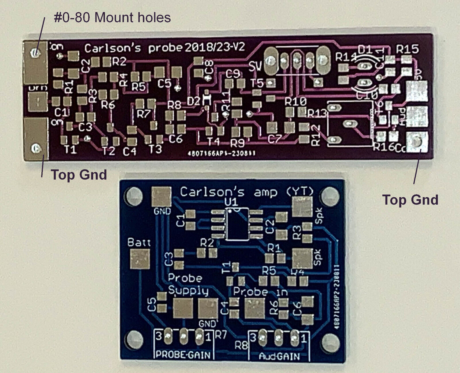
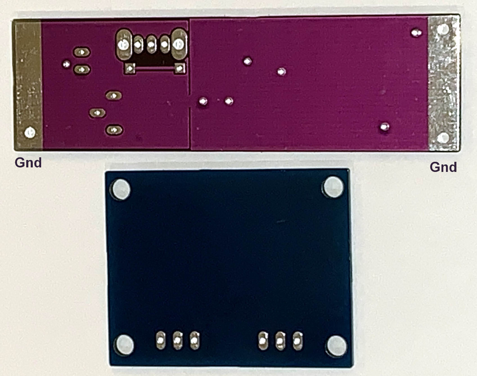
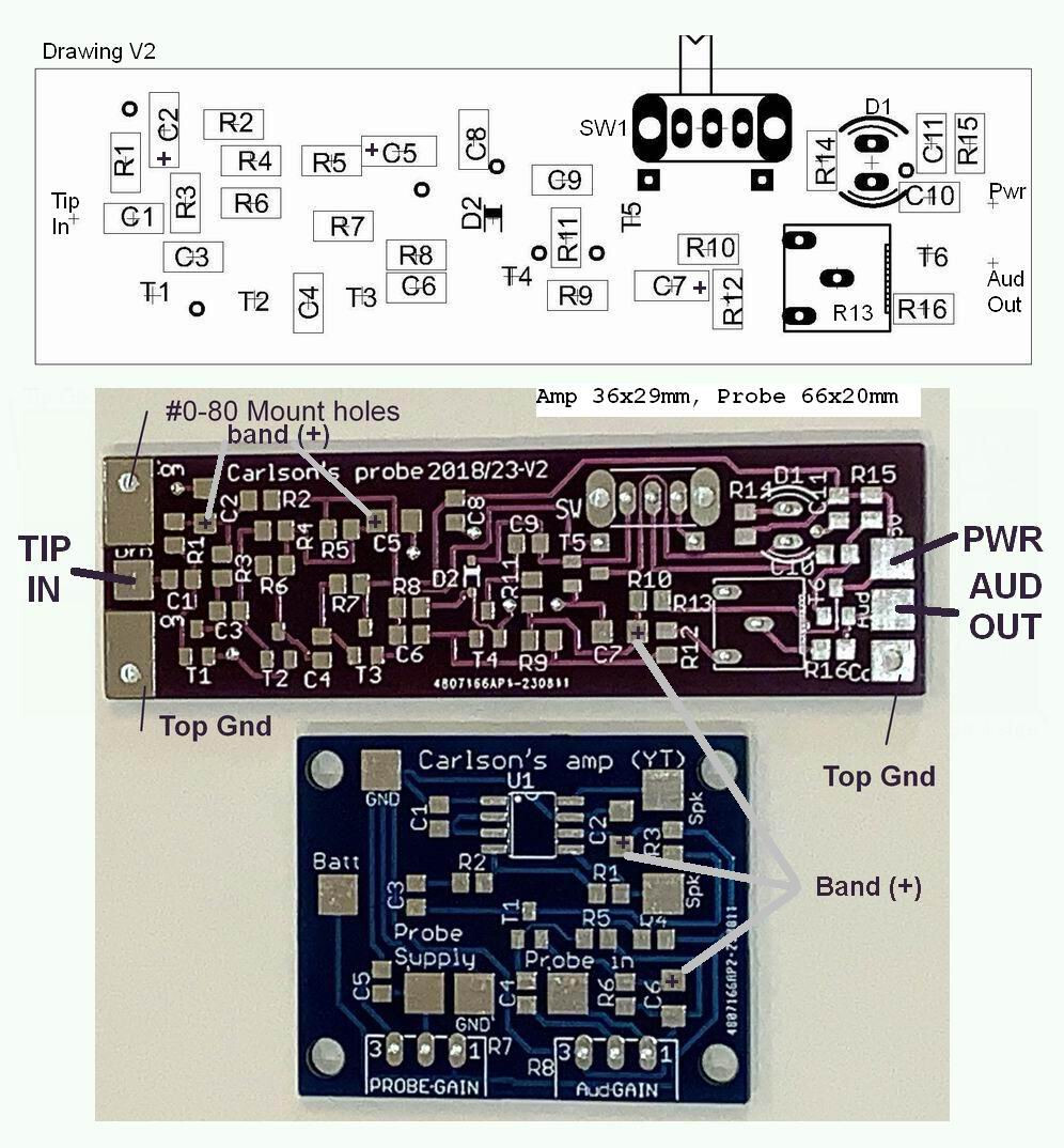
New and Improved Probe PCB with mounting holes & Top-side grounds.
(No affiliation with Mr Carlson's Lab)
As seen on YouTube and commented on on many other sites, Paul Carlson designed a very useful non-contact very high gain electronic probe for investigating just about any kind of electrical signal from audio to RF. The design is well proven and open-sourced. There are also several open-source PCB designs for the probe and amplifier, but most of them are SMD designs. This is likely the primary barrier to building a one-off implementation of this design. To address this, we used an open-source version of the PCB design by Yannick99 at www.instructables.com. These 2 PCBs are well designed and reliable, and used in many DIY probes.Anyone interested in building the probe should first review:
Carlson's YouTube video @ https://www.youtube.com/watch?v=uVkJqqZroN0
Yannick99 @ https://www.instructables.com/Carlsons-Super-Probe/
Web search for many other reviews and assembly hints.
Here is a great UT video of Carlson using the SuperProbe to locate a noisy component inside a complex transceiver. He makes it seem so easy, and with the SuperProbe it is! https://www.youtube.com/watch?v=uiK1BD7HILo
The PCBs
This kit includes only the main PCBs with NO PARTS. There are many components needed to construct a complete probe and amplifier. While there are a few through-hole & panel mounted components, all of the remaining parts are 0805/1206 SMD parts. Soldering such components requires specific equipment, soldering tools, solder, tweezers, optics, skill and patience. We will provide the same instructions that come with our complete parts kit, but you are responsible for sourcing everything. Schematic details are included and are identical to the original design These PCBs REQUIRE ASSEMBLY.The Assembly
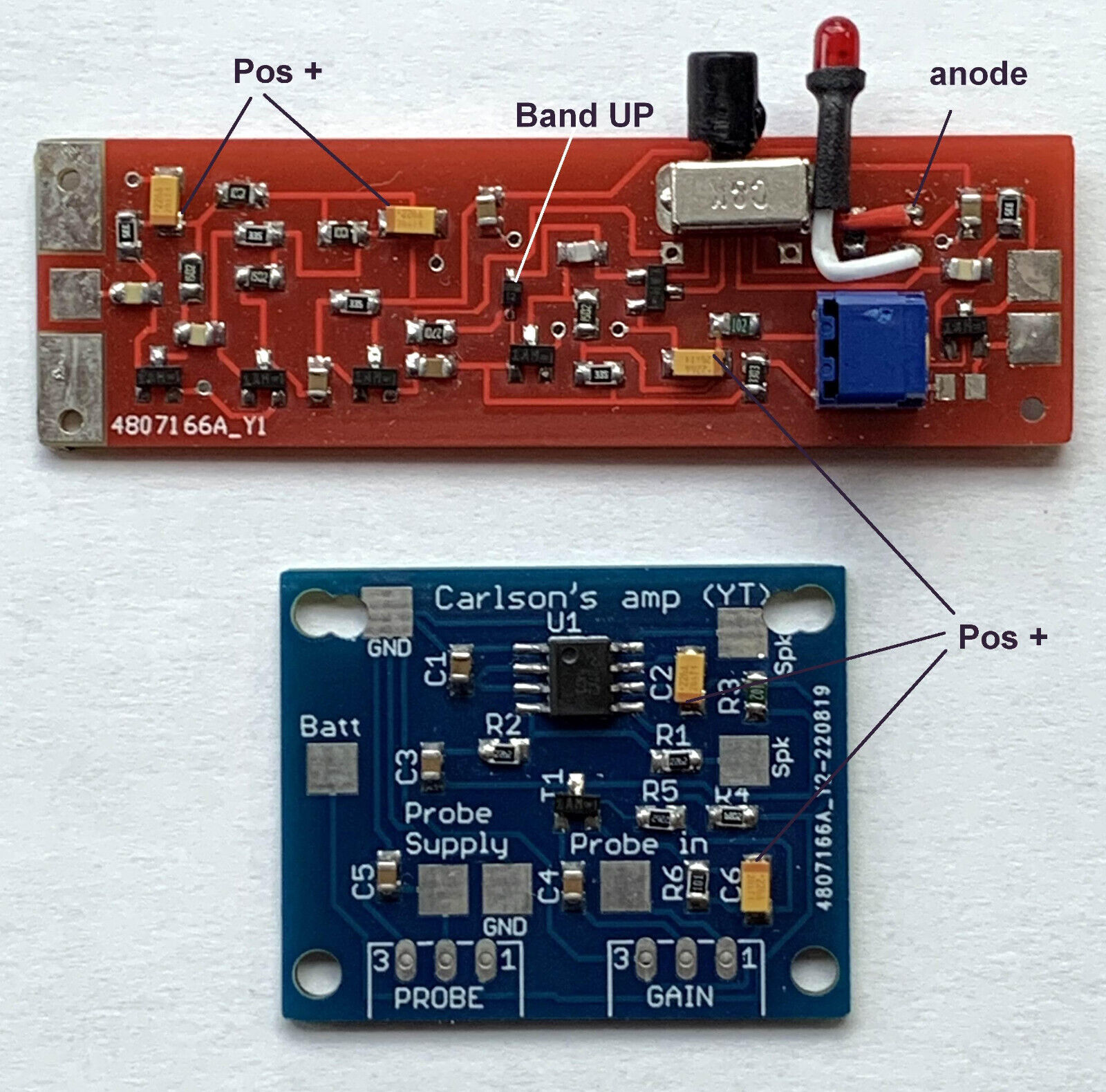
While there are a few through-hole & panel mounted components, all of the remaining parts are 0805/1206 SMD parts. Soldering such components requires specific equipment, soldering tools, solder, tweezers, optics, skill and patience. Follow the included instructions in detail. Schematic details are included and are identical to the original design.Some of the listing photos show a particular implementation in a very compact package. Such compactness is not necessary, but demonstrates what can be achieved. Photos may include components not on the bill-of-material, and are included as suggestions for completing the probe.
See Our Battery Pack Option Too
Check our listing for a Li-Ion battery pack & charger. eBay #166266862893https://www.ebay.com/itm/166266862893
Parts List:
Two (2) PCBs ONLY.Sale Particulars
Buyers Note:eBay collects 12-25% of the final price of every transaction on this platform, so it is an expensive place to run a small business. We try to provide a good value to customers anyhow. This kit is available elsewhere on the web at a lower cost and with free shipping. But due to eBay policies you have to find it your self. Warranty return is 30 days, buyer pays return shipping.
Flat First Class (GA) Shipping with Tracking.
Ask questions before ordering.